Boost converter design Switch mode power supply What is a boost converter? basics, working, design & operation
The boost converter in the design example. | Download Scientific Diagram
Converter upcoming
Design and implement of boost converter.
Design of a new boost converterProposed boost converter What is boost converter? basics, working, operation & design of dcEmerging technologies: boost converter design.
Boost proposedPfc converter stepping inductor 2mh Boost converter mosfet current off gif electronics path inductor attachment circuits operation learnaboutDesign a boost converter.
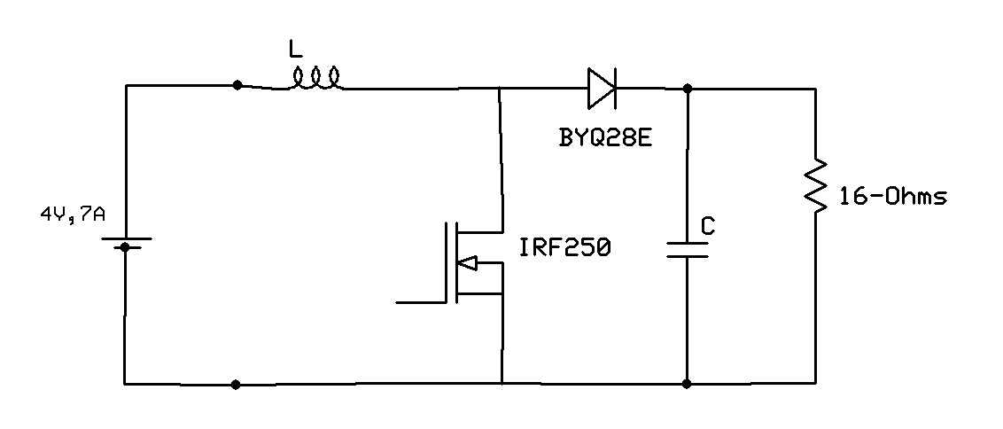
![What is Boost Converter? Basics, Working, Operation & Design of DC](https://i2.wp.com/components101.com/sites/default/files/components/Boost-Converter.png)
Converter schematic
Schematic of the new boost converterBoost converter Pfc boost circuit converter using power factor correction critical conduction mode workingBoost converter components choose schematic circuitlab created using.
Converter boostBoost converter example Boost converter schematicBoost converter pcb layout.
![What is a Boost Converter? Basics, Working, Design & Operation](https://i2.wp.com/components.monofindia.com/wp-content/uploads/2021/06/1-12-300x203.jpg)
Schematic of the tested boost converter configuration.
Converter inductor converters basicsThe boost converter in the design example. Schematic of the boost converter under study.The boost converter in the design example..
Power factor correction (pfc) – working of pfc boost converter usingConverter boost dc fig 300w off-line power factor correction (pfc) boost converterBoost converter.
![What is a Boost Converter? Basics, Working, Design & Operation](https://i2.wp.com/components.monofindia.com/wp-content/uploads/2021/06/4-5.jpg)
The boost converter design
Operation electricaltechnology monofindia components latches components101What is a boost converter? basics, working, design & operation Boost schematicHow to choose components for boost converter.
Converter schematic switching regulator .
![Design of a new boost converter | Download Scientific Diagram](https://i2.wp.com/www.researchgate.net/publication/270318272/figure/fig2/AS:341326504710189@1458389989128/Design-of-a-new-boost-converter.png)
![Schematic of the new boost converter | Download Scientific Diagram](https://i2.wp.com/www.researchgate.net/profile/Jose_Cobos/publication/224324034/figure/download/fig3/AS:667708437827589@1536205505165/Schematic-of-the-new-boost-converter.png)
![Boost Converter Design](https://i2.wp.com/www.simonbramble.co.uk/dc_dc_converter_design/boost_converter/boost_converter.png)
![EMERGING TECHNOLOGIES: BOOST CONVERTER DESIGN](https://3.bp.blogspot.com/-_c7r4X_t3Z0/VWhx4R3xS6I/AAAAAAAABAY/BuGdrnemRmg/s1600/BOOST%2BCONVERTER%2BBLOG.bmp)
![The boost converter in the design example. | Download Scientific Diagram](https://i2.wp.com/www.researchgate.net/profile/George_Weiss/publication/3279632/figure/download/fig1/AS:670705007988744@1536919943741/The-boost-converter-in-the-design-example.png)
![Boost converter](https://i2.wp.com/image.slidesharecdn.com/boostconverter-140324051808-phpapp02/95/boost-converter-18-1024.jpg?cb=1395638329)
![The boost converter design | Download Scientific Diagram](https://i2.wp.com/www.researchgate.net/profile/Saeed_Mohsen/publication/340690655/figure/fig5/AS:881440539545600@1587163209933/The-boost-converter-design.png)
![Design a boost converter | All About Circuits](https://i2.wp.com/forum.allaboutcircuits.com/proxy.php?image=http:%2F%2Fwww.learnabout-electronics.org%2FPSU%2Fimages%2Fboost-converter-cct02.gif&hash=de9644f2f8e0f1c048950052ae3834ff)
![Boost_converter_analysis_2_13_12.mp4 - YouTube](https://i.ytimg.com/vi/qBCld7j_E2c/maxresdefault.jpg)